Kicad 4 Layer Pcb
Then, the layer situation of this component will be shown in the pcb design graphic. [stuart patterson] presents his guide for advanced pcb graphics in kicad 6.0 and inkscape, (video, embedded below) to help you on your way to that cool looking pcb build.
Kicad Flex Pcb PCB Designs
In printed circuit boards, you will hear the term “layers” quite a bit.

Kicad 4 layer pcb. I couldn't get to work the edge.cuts layer in inkscape (same problem as him), so since it was a simple 85.6x54 mm card with edges of 2.5 mm radius. There have been many important changes that make this. Kicad 6.0 roadmap this document is the kicad version 6 developer's road map document.
Features of the 4 layer board. Kicad eda (43) 4.7 out of 5. Tools like eeschema, kicad, pcbnew, gerbview, pi editor, pcb calculator, bitmap2component.
Go to view > 3d view and turn on preference > realistic mode. Im jahr 1992 wurde kicad erstmals veröffentlicht. I easily drew them in kicad in the edge.cuts layer.
1) reference plane, impedance calculation can be done. Kicad supports an integrated design workflow in which a schematic and corresponding pcb are designed together, as well as standalone workflows for special uses. See the kicad download page for guidance.
You can even select the text tool and the b.silks layer to put your name on your pcb: You can change the number of layers. Finally, a truly impressive board made with kicad is crazyflie (figure 5.12).
This is part of a series of short tutorials on advanced topics of using kicad, the favorite schematic/pcb design software here at wayne and layne. It’s popular among different users from students to professionals. Library maintainer rules & guidelines.
Kicad can be considered mature enough to be used for the successful development and maintenance of complex electronic boards. The shape is specifically designed to implement the drone’s body and arms. The kicad project is proud to announce the release of version 6.0.0.
Now, with a normal pcb, you would want to add some mounting holes. The board implements the flight controller of a tiny drone. It features schematic capture, integrated circuit simulation, printed circuit board (pcb) layout, 3d rendering, and plotting/data export to numerous formats.
Choose where you want to save your project and type in a name for it. In 2012 wurde das dateiformat für boards und damit die dateiendung von „.brd“ auf „.kicad_pcb“ umgestellt. Kicad binaries are available for download for windows, macos, and linux or will be in the very near future.
Volume discount for prototype and 4 layer 40% price reduction ships in. We have already given you a basic idea of what this software is and the kinds of tools it offers, but we shall talk about those things in more detail. Ultiboard is printed circuit board design and layout software that integrates seamlessly with multisim to accelerate pcb prototype development.
This is the first major version release of kicad since 5.0.0 was released in july of 2018. If a component is on the bottom layer of a pcb, double click the component display and set its layer in component properties. Drag and drop your kicad, eaglecad, or zipped gerber files.
4 layer pcb board has gnd and power layers in the middle of top and bottom layers. ※kicad ver.4 をご利用の方はこちらをご確認ください。 p板.comでは、kicad より出力したガーバーデータで数々の製造実績がありますので、出力したガーバーデータで安心してご発注いただけます。 step 1 データ作成準備. Plot your kicad pcb as gerber files.
It features an integrated environment for schematic capture, pcb layout, manufacturing file viewing, spice simulation, and engineering calculation.tools exist within the package to create bill of materials, artwork, gerber. Visualizing layer structures — pcb designers can. All boards are manufactured in the united states including 2 and 4 layer rigid pcbs with our classic purple soldermask as well as 2 layer flex pcbs and 2 layer rigid with black substrate and clear mask which we call after dark.
Electroless plating is widely used in the printed circuit board (pcb) production and processing which has holes on that and it can also be called pth(plate through hole), the main purpose is to deposit a layer of copper through a series of chemical treatment methods in the conductive substrate,. We directly accept kicad board files when ordering. Once i had everything finished.
While you may hear a pcb being referred to as a “single layer pcb” and think of it in terms as in reality, even a single layer pcb contains multiple layers of material in order to operate correctly. This unique approach is based on a powerful software engine that allows you to capture circuits, design circuit boards and layouts. Click design and select layer stack manager.
The goal of this document is to provide an overview for developers of the goals for the project for the version 6 release of kicad. Top dielectric and bottom dielectric must be ticked if the pcb has two layers. It is living document that should be maintained during the version 6 development cycle.
From here, you can open or create new projects. When you open up kicad, you’ll see the window shown in image 2.1. Ultiboard software offers efficient pcb design layout and routing with a customizable environment.
These can be 2 layer pcb, 4 layer pcb, and so forth. If you learn to use altium software to draw 4 layer boards, you can also use easyeda, eagle, and kicad to draw 4 layer boards. Kicad eda is a combination of many other tools incorporated to provide various functionalities to users.
Turn up all the settings you want, set your background color, and you'll have a nice render of your pcb! ——technical analysis of plating copper for pcb processing. It facilitates the design and simulation of electronic hardware.
A copper pour or fill refers to an area on a printed circuit board where the original copper is not etched away, and remains in place, usually electrically connected to the ground signal, producing a “ground plane”. Designspark pcb is a very popular and easy to learn free pcb design tool for capturing circuits and arranging printed circuit boards for electronic design automation.
4Layer PCB Design in KiCad 5 Quick Thoughts Paul Bupe, Jr

Kicad GPL PCB Suite

4layer pcb, need via to connect 2nd layer only Footprints KiCad.info Forums

Kicad For 4 Layer Rigid / 2 Layer Flex Design Layout KiCad.info Forums

4Layer PCB Design in KiCad 5 Quick Thoughts Paul Bupe, Jr

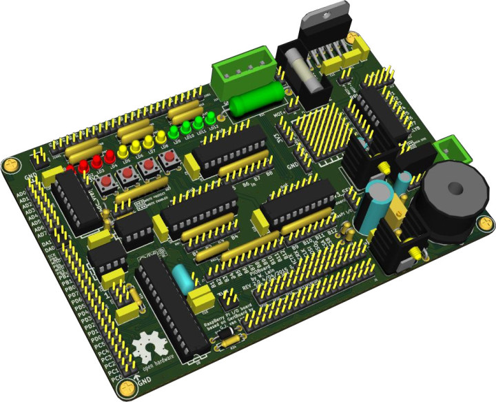
Kicad On Raspberry Pi 4 Circuit Boards
KiCad Tutorial How to make a 4 layer PCB in KiCad YouTube

4 Layer Pcb Design Tutorial Kicad PCB Designs

4 Layer Pcb Design Tutorial Kicad PCB Designs
KiCAD circuit 2W PCB Design TL071+ TBA820M +CD4016BMT // 4 Layers YouTube

4Layer PCB Design in KiCad 5 Quick Thoughts Paul Bupe, Jr

Designing a Functional Testing PCB part 2/x KiCad 4 Layer PCB YouTube

4 Layer Pcb Kicad PCB Designs

KiCad PCB (kicad_pcb) تويتر
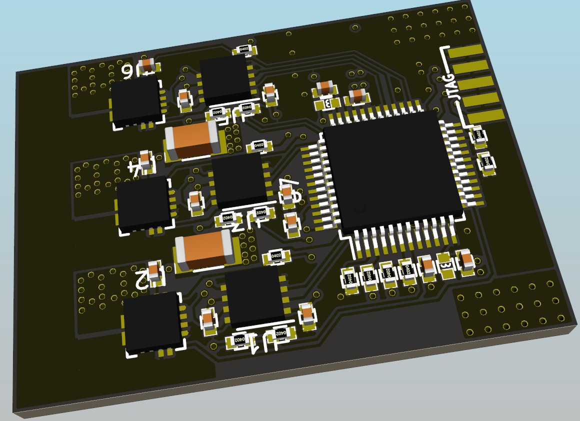
4Layer PCB Design in KiCad 5 Quick Thoughts Paul Bupe, Jr

Kicad On Raspberry Pi 4 Circuit Boards
KiCAD PCB 4 Layer Swapping & Stackup Utreon

No Copper Fill for Inductor On All Layers (4 layer design) Layout KiCad.info Forums

4 Layer Pcb Design In Orcad PCB Designs